PCB Design Showcase
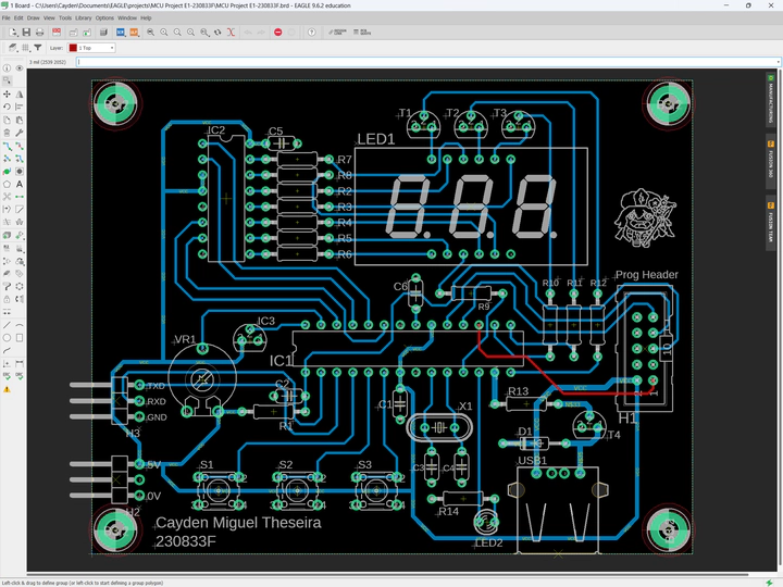 Image credit: Cayden Miguel Theseira
Table of Contents
Project Scope
The aim of this project was to design and implement a 4-layer printed circuit board (PCB) using Autodesk Eagle software. The objective was to create an efficient, noise-managed, and compact PCB while maintaining a functional and aesthetically organized design.

My Role
I was responsible for the entire PCB development process, including schematic design, component placement, layer routing, and final layout. I also conducted design rule checks (DRC) and oversaw soldering and assembly to ensure proper functionality.
Work Process
Schematic Design
- Created logical connections between components.
- Verified schematic accuracy to avoid errors.

Component Placement
- Positioned components to minimize trace lengths and optimize performance.
Layer Routing
- Top and Bottom Layers: Used for signal traces.
- Inner Layers: Reserved for power and ground planes to reduce interference.
Design Rule Check (DRC)
- Ensured compliance with trace widths, clearances, and component placements.
Assembly and Testing
- Used soldering tools to populate the board and test its functionality.
Outcome Achieved
The project was successful in achieving its goals of creating a functional and professional 4-layer PCB using Autodesk Eagle.
Key Takeaways:
- Gained practical knowledge of component integration and the stages of PCB manufacturing.
- Deepened understanding of the importance of proper PCB design standards.
- Enhanced technical skills and exposure to real-world applications.
Board Highlights:
Op Amp Circuit
- The op-amp circuit is integral for signal amplification and conditioning in this project.
Schematic
Board Layout

MCU Integration
- The microcontroller unit (MCU) is the brain of the system, responsible for processing inputs and controlling outputs.
Schematic

Board Layout

Challenges and Solutions
- Trace Routing Complexity: Solved by utilizing 4 layers to isolate signals and reduce interference.
- Component Placement: Balanced performance and aesthetics through careful organization.
- Layer Optimization: Dedicated inner layers to power and ground planes to enhance efficiency and reduce noise.
Conclusion
This project demonstrates my expertise in PCB design using Autodesk Eagle. By combining technical precision with a clean layout, I achieved a functional and professional 4-layer PCB. The board is ready for testing and further integration into larger systems.